08 Feb 2023
In this work, the threshold voltage instability of normally-off p-GaN high
electron mobility transistors (HEMTs) has been investigated by monitoring the
gate current density during device on-state. The origin of the gate current
variations under stress has been ascribed to charge trapping occurring at the
different interfaces in the metal/p-GaN/AlGaN/GaN system. In particular,
depending on the stress bias level, electrons (VG < 6 V) or holes (VG > 6 V)
are trapped, causing a positive or negative threshold voltage shift {DVTH,
respectively. By monitoring the gate current variations at different
temperatures, the activation energies associated to the electrons and holes
trapping could be determined and correlated with the presence of nitrogen
(electron traps) or gallium (hole traps) vacancies. Moreover, the electrical
measurements suggested the generation of a new electron-trap upon long-time
bias stress, associated to the creation of crystallographic dislocation-like
defects extending across the different interfaces (p-GaN/AlGaN/GaN) of the gate
stack.
24 Apr 2020
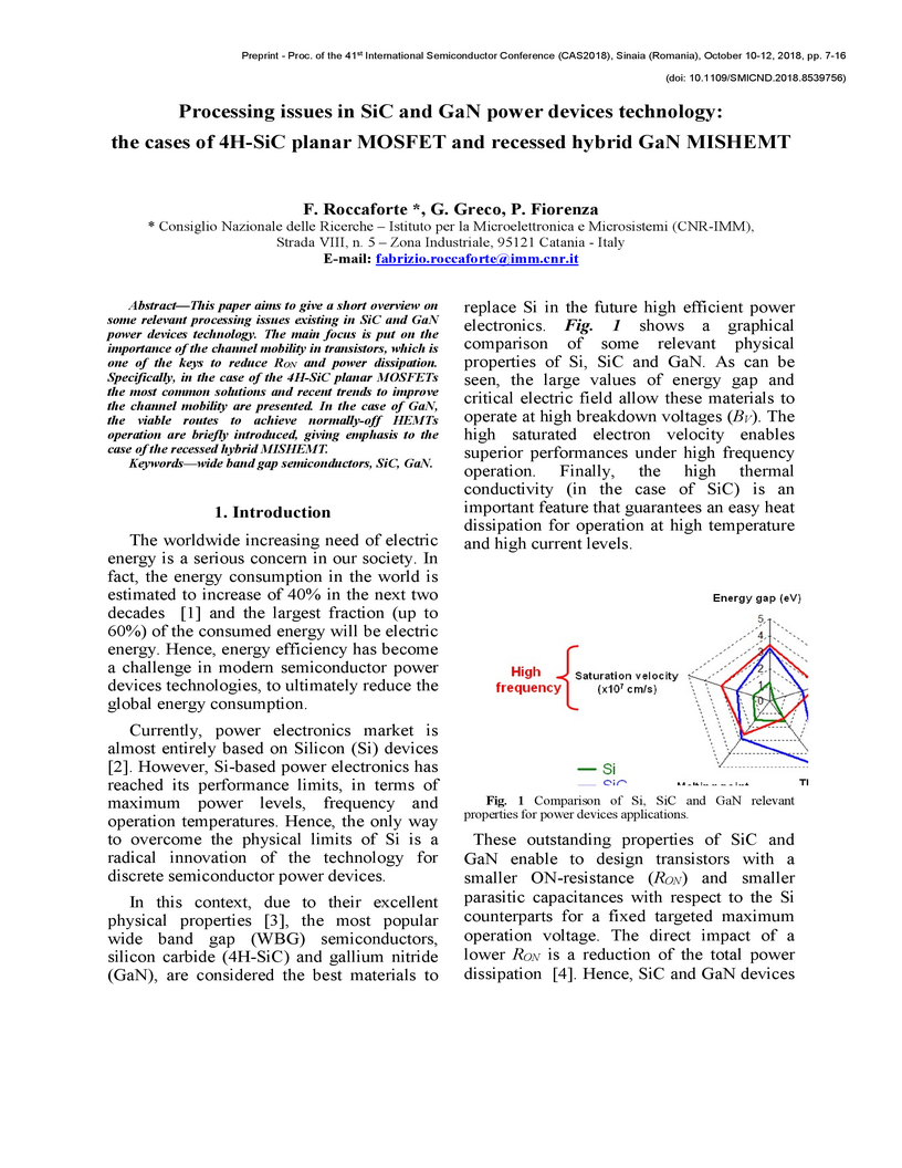
This paper aims to give a short overview on some relevant processing issues
existing in SiC and GaN power devices technology. The main focus is put on the
importance of the channel mobility in transistors, which is one of the keys to
reduce RON and power dissipation. Specifically, in the case of the 4H-SiC
planar MOSFETs the most common solutions and recent trends to improve the
channel mobility are presented. In the case of GaN, the viable routes to
achieve normally-off HEMTs operation are briefly introduced, giving emphasis to
the case of the recessed hybrid MISHEMT.
There are no more papers matching your filters at the moment.
