Ask or search anything...
Real-Time Recurrent Reinforcement Learning
13 Mar 2025 julian lemmel
We introduce a biologically plausible RL framework for solving tasks in
partially observable Markov decision processes (POMDPs). The proposed algorithm
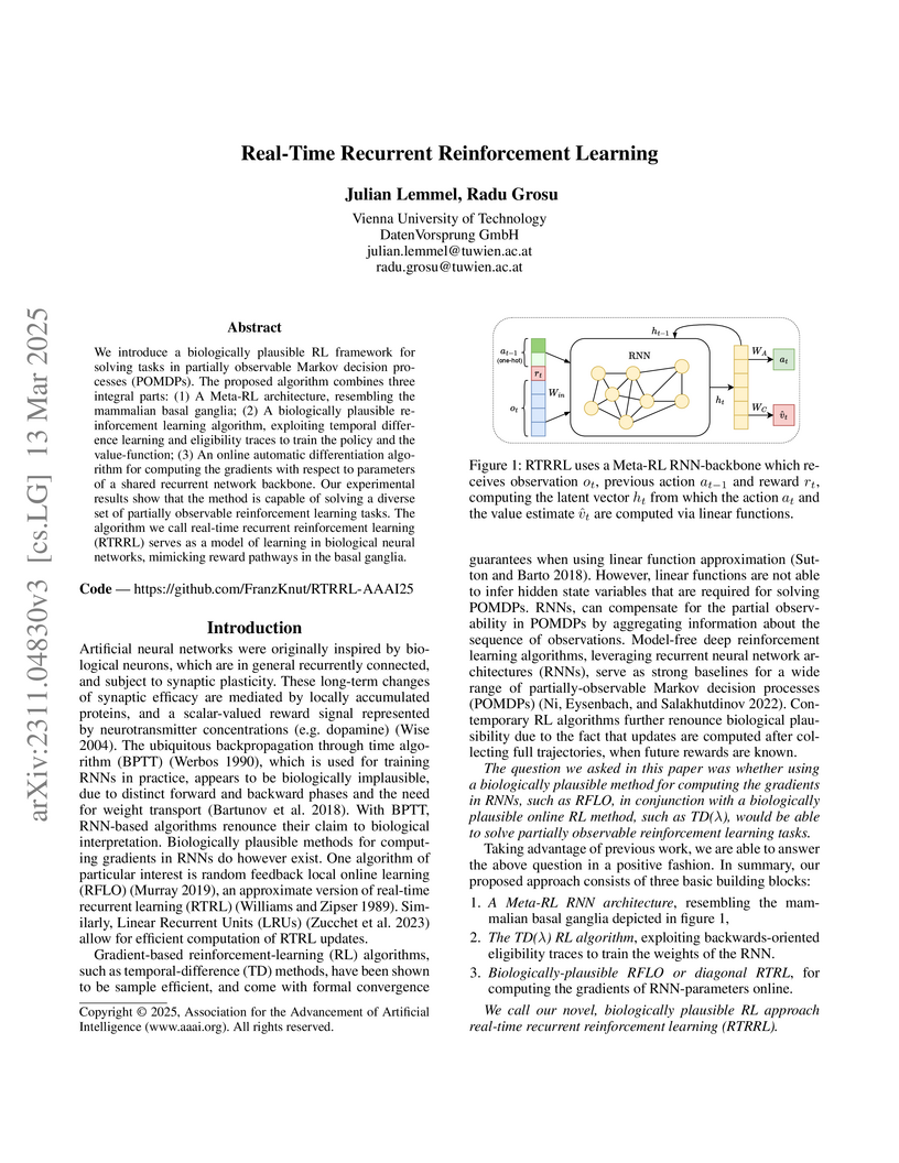
combines three integral parts: (1) A Meta-RL architecture, resembling the
mammalian basal ganglia; (2) A biologically plausible reinforcement learning
algorithm, exploiting temporal difference learning and eligibility traces to
train the policy and the value-function; (3) An online automatic
differentiation algorithm for computing the gradients with respect to
parameters of a shared recurrent network backbone. Our experimental results
show that the method is capable of solving a diverse set of partially
observable reinforcement learning tasks. The algorithm we call real-time
recurrent reinforcement learning (RTRRL) serves as a model of learning in
biological neural networks, mimicking reward pathways in the basal ganglia.
Hysteresis Measurements as a Diagnostic Tool: A Systematic Approach for Stability Benchmarking and Performance Projection of 2D-Materials-Based MOSFETs
25 Sep 2025
 Peking University
Judging by its omnipresence in the literature, the hysteresis observed in the transfer characteristics of emerging transistors based on 2D-materials is widely accepted as an important metric related to the device quality. The hysteresis is often reported with attributes like "negligible" or "small" without giving any specifics as to how this was determined and against what reference the measured values were compared to. Quite surprisingly, there appears to be only a fragmentary understanding of the mechanisms actually contributing to hysteresis and the sensitivity of the actual measurement on various experimental parameters. We attempt to close this gap by first providing a comprehensive theoretical analysis of the dominant mechanisms contributing to hysteresis: charge trapping by defects from the channel or the gate, the drift of mobile charges, and eventually ferroelectricity. We continue by suggesting methods to experimentally distinguishing between these phenomena. Based on these discussions it becomes clear that previously reported hysteresis values have little meaning as they have been non-systematically recorded under arbitrary conditions. In order to resolve this predicament, we propose a standardized hysteresis measurement scheme to establish the hysteresis as a comparable metric for the assessment of device stability. Our standardized scheme ensures that hysteresis data can be effectively compared across different technologies and, most importantly, provide a means to extrapolate data obtained on thicker prototypes to subnanometer equivalent oxide thicknesses. This facilitates the systematic benchmarking of insulator/channel combinations in terms of stability, which thereby enables the screening of material systems for more stable and reliable 2D-material-based MOSFETs.
ASP(AC): Answer Set Programming with Algebraic Constraints
10 Aug 2020
Weighted Logic is a powerful tool for the specification of calculations over semirings that depend on qualitative information. Using a novel combination of Weighted Logic and Here-and-There (HT) Logic, in which this dependence is based on intuitionistic grounds, we introduce Answer Set Programming with Algebraic Constraints (ASP(AC)), where rules may contain constraints that compare semiring values to weighted formula evaluations. Such constraints provide streamlined access to a manifold of constructs available in ASP, like aggregates, choice constraints, and arithmetic operators. They extend some of them and provide a generic framework for defining programs with algebraic computation, which can be fruitfully used e.g. for provenance semantics of datalog programs. While undecidable in general, expressive fragments of ASP(AC) can be exploited for effective problem-solving in a rich framework. This work is under consideration for acceptance in Theory and Practice of Logic Programming.
Performance and reliability potential of BiOSe/BiSeO transistors
11 Dec 2025
While 2D materials have enormous potential for future device technologies, many challenges must be overcome before they can be deployed at an industrial scale. One of these challenges is identifying the right semiconductor/insulator combination that ensures high performance, stability, and reliability. In contrast to conventional 2D interfaces, which suffer from van der Waals gaps or covalent bonding issues, zippered structures such as the high-mobility 2D semiconductor BiOSe and its native high- oxide BiSeO offer high-quality interfaces, good scalability, and excellent device performance. While most prior work has focused mainly on basic device behavior, here we also thoroughly assess the stability and reliability of this material system using a multiscale approach that integrates electrical characterization, density functional theory, and TCAD simulations, linking atomistic states to device-scale reliability. By analyzing four transistor design generations (top-gated, fin, and two gate-all-around FETs), we provide realistic predictions for how this system performs at the ultimate scaling limit. We identify oxygen-related defects in the oxide as the main contributors to hysteresis and recoverable threshold shifts, and we propose mitigation strategies through encapsulation or oxygen-rich annealing. Benchmarking the extracted material parameters against IRDS 2037 requirements, we demonstrate that BiOSe/BiSeO transistors can achieve high drain and low gate currents at ultra-scaled conditions. These findings position this material system as a technologically credible and manufacturing-relevant pathway for future nanoelectronics.
Assessing the Feasibility of Developing a Federated ERP System
01 Sep 2011
In past years ERP Systems have become one of the main components within the
corporate IT structure. Several problems exist around implementing and
operating these systems within companies. In the literature one can find
several studies about the problems arising during the implementation of an ERP
system. The main problem areas are around the complexity of ERP systems. One
vision to overcome some of these problems is federated ERP. Federated ERP
systems are built of components from different vendors, which are distributed
within a network. All components act as one single ERP system from the user
perspective. The decreased complexity of such a system would require lower
installation and maintenance cost. Additional, only the components which are
needed to cover the company's business processes would be used. Several
theories around this concept exist, but a feasibility assessment of developing
a federated ERP system has not been done yet. Based on a literary analysis of
existing methods for feasibility studies, this paper is applying strategic
planning concepts and referential data from the traditional ERP development to
provide a first assessment of the overall feasibility of developing a platform
for federated ERP systems. An analytical hierarchical approach is used to
define effort and effect related criteria and their domain values. The
assessment as the criteria is done in comparison to the development of a
classical ERP system. Using the developed criteria, a net present value
calculation is done. The calculation of the net present value is done on an
overall, not company specific level. In order to estimate the weighted average
cost of capital, the values from successful software companies are used as a
baseline. Additional potential risks and obstacles are identified for further
clarification.
On Iterated Lorenz Curves with Applications: The Bivariate Case
02 Jul 2025
It is well known that a Lorenz curve, derived from the distribution function of a random variable, can itself be viewed as a probability distribution function of a new random variable [2]. In a previous work of ours [3], we proved the surprising result that a sequence of consecutive iterations of this map leads to a non-corner case convergence, independent of the initial random variable. Namely, the limiting distribution follows a power-law distribution. In this paper, we generalize our result to the bivariate setting. We do so using Arnold's type definition [2] of a Lorenz curve, which offers the greatest parsimony among its counterparts. The situation becomes more complex in higher dimensions as the map affects not only the marginals but also their dependence structure. Nevertheless, we prove the equally surprising result that under reasonable restrictions, the marginals again converge uniformly to a power-law distribution, with an exponent equal to the golden section. Furthermore, they become independent in the limit. To emphasize the multifaceted nature of the problem and broaden the scope of potential applications, our approach utilizes a variety of mathematical tools, extending beyond very specialized methods.
ZFK := ZFC with a Complement, or: Hegel and the Synto-Set-Theory
30 Jul 2008
What is the slightest modification of ZF to add a complement-axiom? The answer in my Ph.D. thesis 1971 was ZF'': Zermelo-Fraenkel with replacement for only well-founded domains and an omega-axiom. In 1974, Alonzo Church published a similar system, as did Urs Oswald in 1976. In his 1976 Ph.D. thesis, E. Mitchell also designed, a system very similar to ZF''. In this article we argue that ZF'' is the slightest modification of ZF among all these systems and that its successor ZFK is the simplest set theory with a universal set at all.
Classical Concepts in Quantum Programming
29 Apr 2003
The rapid progress of computer technology has been accompanied by a
corresponding evolution of software development, from hardwired components and
binary machine code to high level programming languages, which allowed to
master the increasing hardware complexity and fully exploit its potential.
This paper investigates, how classical concepts like hardware abstraction,
hierarchical programs, data types, memory management, flow of control and
structured programming can be used in quantum computing. The experimental
language QCL will be introduced as an example, how elements like irreversible
functions, local variables and conditional branching, which have no direct
quantum counterparts, can be implemented, and how non-classical features like
the reversibility of unitary transformation or the non-observability of quantum
states can be accounted for within the framework of a procedural programming
language.
There are no more papers matching your filters at the moment.